What is Register Transfer Notation?
This article assumes an understanding of Von Neumann computer architecture and assembly language.
Register Transfer Notation (RTN) is a mathematical notation that describes how data moves between registers in a CPU. It is often used to describe how CPU instructions work internally. That is, the sequence of steps performed to execute an instruction.
The following are some symbols that are used in RTN. These are not all of the symbols available but are some of the common ones:
- ← A left pointing arrow symbol means data is being copied to whatever is on the left
For example, this means move the number 5 into the MAR register:
MAR ← 5
- [MAR] - square brackets around the name of a register means retrieve the content of the register
- [[MAR]] - double square brackets around the name of a register means the register contains the memory address from which the contents should be retrieved
CPU registers can be more than one byte in length. Rounded brackets after the register name are used to refer to only part of a register. If we had a two byte register, the symbol “L” (for lower) might be used to refer to one of the two bytes and the symbol “H” (for high) might refer to the other. Exactly which byte is which might vary with the CPU design.
- [MAR(H)] would retrieve only one of the two bytes contanied within the MAR register and [MAR(L)] would retrieve the other.
For an example of Register Transfer Notation, let’s consider a fictional CPU which has a single general working register called the accumulor or ACC for short. It has an instruction called LDD which loads a number from a specified memory location into the ACC register. Let’s say we are executing LDD FE, that is we want an instruction to load whatever is at memory address hexadecimal FE into the accumulator.
Say we have a CPU with a 16-bit data bus which is capable of loading two bytes from memory at once. The instruction consists of the opcode LDD, which we will say is one byte in length, and is followed by the operand which is a memory address of hexadceimal FE that is also one byte long. Hence the instruction is two bytes in length and so the CPU can load this particular instruction in one step. Some instructions with longer operands might require more than one step to load.
The following RTN describes how the LDD instruction may work internally. This kind of description is an example of a fetch/execute cycle for an instruction. CPUs are continuously in fetch/execute cycles, retrieving instructions from memory and then running them.
MAR ← [PC]
MDR ← [[MAR]]
CIR ← [MDR]
MAR ← [MDR(L)]
ACC ← [[MAR]]
PC ← [PC] + 2
Let’s explain this step by step:
MAR ← [PC] - Firstly the content of the Program Counter or PC register (which tells us the memory location we are currently at in the program) is loaded into the special Memory Address Register (MAR). The MAR is used to temporarily hold the memory address that we want to retrieve from memory next.
MDR ← [[MAR]] - The contents of the memory address referred to by the MAR (that we just loaded) is retrieved and this is placed into the Memory Data Register. As we have a 16-bit CPU we have been able to retrieve two bytes in this step. This is the LDD instruction (a one byte opcode) and it’s operand (a second byte). The operand for LDD instruction is a memory address from which we will retrieve the data we want to send to the accumulator register.
CIR ← [MDR] - The contents of the MDR (the LDD instruction opcode and its operand) are copied into the Current Instruction Register, which as the name implies stores the current instruction.
MAR ← [MDR(L)] - We said the LDD instruction consisted of two bytes. The opcode for LDD was in one byte and the operand (hex FE) was in the other byte. Let’s assume the lower byte (L) is the operand. Here we move the operand into the MAR. This is in preparation for getting the contents of this address.
ACC ← [[MAR]] - Now the content of the address pointed to by the MAR register is retrieved from memory and placed into the accumulator general purpose register. The instruction execution is now complete.
PC ← [PC] + 2 - Most CPUs have a feature to automatically advance the Program Counter onto the next instruction when the current instruction is complete. So we add 2 to skip over the current instruction which consisted of a 1 byte opcode + a 1 byte operand = 2 bytes. This finds the beginning of the next instruction. Instructions on some CPUs can vary in length and the CPU will vary how far it advances the Program Counter depending on the length of the instruction just executed.
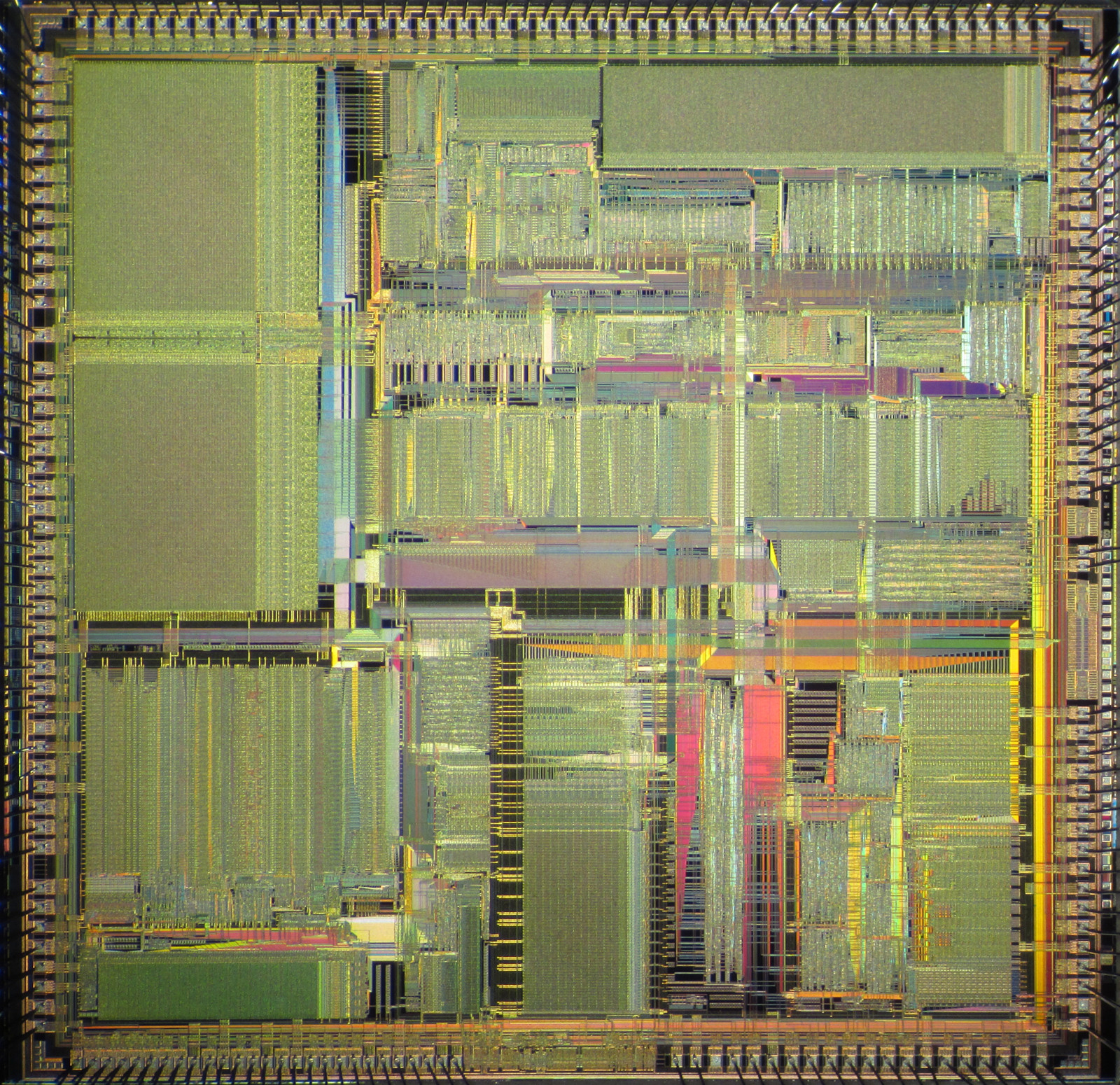
Chip die photo by Pauli Rautakorpi
