How Logic Gates are Built from Transistors
This article assumes an understanding of electronic logic gates. More about the subject can be found in this article:
If we recall the function of an AND logic gate:

It has a truth table like this:
| Input A | Input B | Output |
|---|---|---|
| 0 | 0 | 0 |
| 0 | 1 | 0 |
| 1 | 0 | 0 |
| 1 | 1 | 1 |
So this means the output of the gate is "1" only when both of the inputs are at "1".
If we now look at the following circuit consisting of a lamp and two switches. The switches are in series in the path to the lamp. The lamp will only light when both switches are pressed. If only one switch is pressed the lamp will not light.

If we consider the switches to be the inputs and the lamp the output, the circuit behaves like an AND gate.
Now let's take a look at an OR gate.

The truth table for the OR gate is as follows:
| Input A | Input B | Output |
|---|---|---|
| 0 | 0 | 0 |
| 0 | 1 | 1 |
| 1 | 0 | 1 |
| 1 | 1 | 1 |
OR gates output a "1" if either or both of inputs are "1".
We could rearrange the circuit like this to behave like an OR gate:

The bulb will light if either (or both) of the two switches are pressed. This circuit behaves like an OR gate.
Some early computers were made using logic gates constructed out of switches, exactly in the manner above. The switches were turned on and off using an electromagnet, that is an electrically powered magnet, which is made from a coil of wire. When a voltage is applied to the magnet it pushes the switch into the on position. When the voltage is removed, the magnetic field holding the switch in the on position disappears and the switch flips to off by mechanical spring action. So now we have an electrically activated switch. A component that turns on a switch using a electromagnet is called a relay.
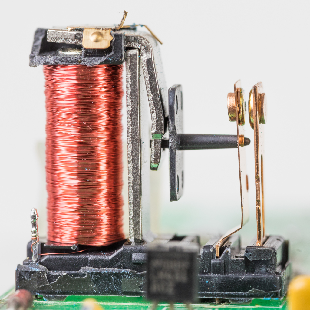
A closeup of a relay is shown below. The electromagnet is the coil of wire on the left and there is a switch on the right. When the magnet activates it pushes the switch contacts together via the metal finger in the centre, then the contacts spring apart when the magnet is off.
There are however problems with using relays for building computers, which include:
- The magnet can only activate the switch quite slowly which puts an upper limit on how fast the computer can operate
- Relays are physically large
- The magnet uses a lot of power to hold the switch on
- As with all things mechanical, relays break after so many thousand activations and need constant replacement.
What we need is an electrically powered switch that is both faster, more reliable and not mechanical.
A transistor is a component that can behave like an electronic switch. Instead of being activated by being physically pressed (either by a finger or a magnet) it is activated by a voltage. The component has three legs. The collector and emitter are like the connections either side of the switch through which the current flows when the switch is pressed. The base defines whether the switch is pressed. If there is a voltage at the base, this is equivalent to the switch being pressed. If there is no voltage then the switch is not pressed.
The electronic symbol for a transistor is show below (left) next to a switch for comparison:

We can replace the switches in the circuit for the AND gate with transistors like this:
Now we can see that only if both of the transistor inputs, A and B, have a voltage applied, will the current flow to cause the lamp to light.
This circuit is almost correct, however if we actually want to build the circuit in practice we need to add some additional components called resistors that restrict the flow of current. These components do not change the logic of how the circuit works at all, but are needed to deal with practical electrical problems that occur when using transistors:

There is a resistor (rectangle symbol) at the base input to each of the transistors because the base can only handle a specific flow of current. If the flow of current is too high, the transistor will be damaged. The resistor limits how much current will flow to the base such that it is within the tolerances of the transistor.
There is a resistor connected between the output of the AND gate and the negative of the battery. This is known as a pull-down resistor and ensures that the output is set to zero (battery negative or ground) when one or both of the transistors are not activated and the AND gate should be outputting a "0". If there were no connection to ground here then the output would be floating when both of the transistors were inactive.
A floating output means that the voltage present is undefined and could be anything. By adding a connection to ground we ensure that the output is definitely zero when the transistors are off. A resistor is needed to prevent a short circuit. In electronics we must never connect the two battery terminals together directly as this causes a large flow of current which would damage the circuit. We can see that if the output were directly connected to ground instead (without the resistor) we would get a short circuit in the situation when both of the transistors were turned on. The resistor limits the current flow to ground.
But what about a NOT gate (inverter)? How does that work?

The inverter can be built with only a single transistor using a circuit like below:
The way this works is when there is a zero at the input, the transistor is switched off and is blocking current from flowing between the collector and emitter. The positive from the battery passes through the top resistor. It cannot go through the transistor and so goes to the output, producing a "1". However, when there in a positive voltage at the input (a "1"), the transistor is activated and current can flow. There is now a path to ground (where electricity prefers to travel) and so the output is now at zero. The resistor at the collector is required to stop the two battery terminals becoming directly connected when the transistor is activated and is called a pull-up (the "up" referring to the positive battery terminal).
Credit: Transistor image by Benedikt.Seidl. Relay image © Raimond Spekking/CC BY-SA 4.0