How to Build a 3-bit Adder Circuit from Logic Gates
This article describes how to construct a 3-bit addition circuit in practice out of logic gates. This circuit can add two binary numbers between 0 and 7. An understanding of how the circuits for full adders and half adders work is assumed.
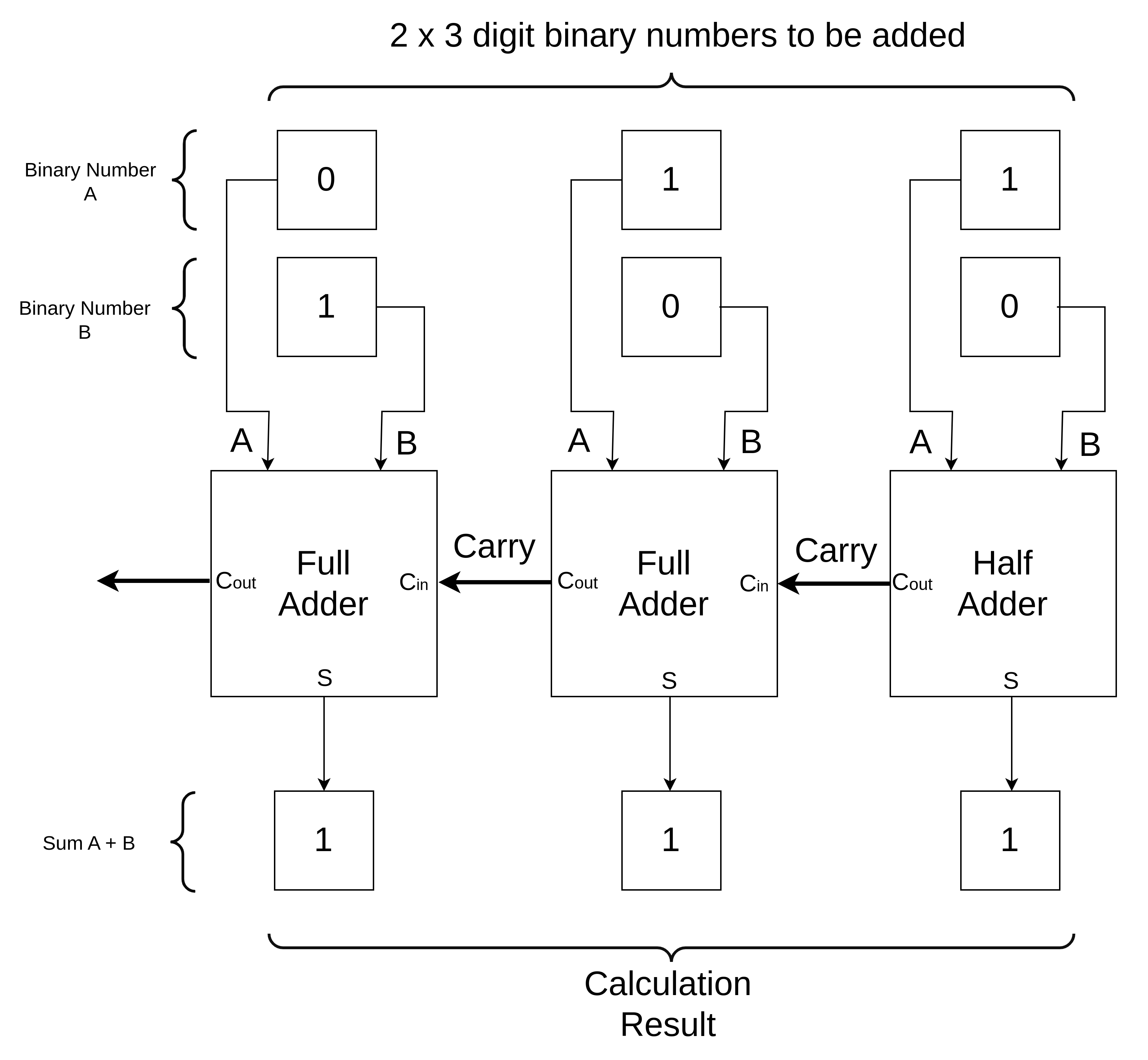
The following is a block diagram of a circuit for adding two 3-bit numbers together. The first pair of bits are added using a half adder (because there is no carry in), then for the next two bits two full adders are needed to handle the bits being added plus any carry from the previous addition.

The block diagram simplifies the circuit by missing out the logic gates. The complete circuit diagram (schematic) is shown below, including all of the logic gates for the full and half adders. The two 3-bit numbers to be added, A and B, are going to be input to the circuit using six switches (at the top of the diagram), with three switches to represent each 3-bit binary number. The output will be displayed on four LEDs (at the bottom) with one for each bit. Four bits of output are needed as 14 (the result of 7+7) requires 4 bits to display.

The circuit is going to use a well-known range of chips for the logic gates called the 7400 series. These chips operate at 5 volts. The output LEDs do not operate at 5V and each LED requires a 169Ω resistor to drop the voltage and also restrict the current to the operating level for the LED.
The logic gates that accept the inputs from the switches should have a logic one (binary digit one) when the switch is pressed and a logic zero (binary digit 0) when the switch is not pressed. The switches are connected to 5V, which signifies logic one. A logic zero is signified by a connection to ground. However, when the switch is not pressed the circuit is disconnected from 5V but ends up not connected to anything as the switch electrically isolates the circuit when not pressed. This is called a “floating” condition and is not a logic zero. When in the floating state (disconnected) a logic gate might do anything at complete random. We need to ensure the gate gets a definitive zero when the switch is not pressed. For this reason the inputs are connected to ground in addition to the switch. So when the switch isolates the path to 5V, there is a path to ground.
We cannot, however, directly connect the inputs to ground. The problem is when the switch is pressed, and 5 volts flows through it, the current would then have an unrestricted path from 5V to ground through that connection. This would be a short circuit and must be avoided in electronics. As you may know from domestic electrics, a short circuit causes the fuse to blow due to the unrestricted flow of current. To solve this we add a restriction in the path to ground, this is what all of the 1KΩ resistors do and are known as “pull-down” resistors. They allow a path to ground to get a well defined logic zero, but not so direct of a path that we would end up with a short circuit when the switch allows 5V to flow in.
The chip part numbers being used are as follows:
- 74LS86 - package of 4x XOR gates
- 74LS08 - package of 4x AND gates
- 74LS32 - package of 4x OR gates
The actual parts purchased may have letters before and after the part number e.g. SN74LS86N, however the only part of the number that is significant to the operation of the circuit is as shown above. There are variations of these chips with different letters between the digits but the “LS” variants must be used for the circuit to work as described. LS stands for “Low-power Schottky” and describes the electrical characteristics of the transistors used within the chip to form the logic gates.
These chips were originally designed in the 1960s but remain in production today and are still widely used.
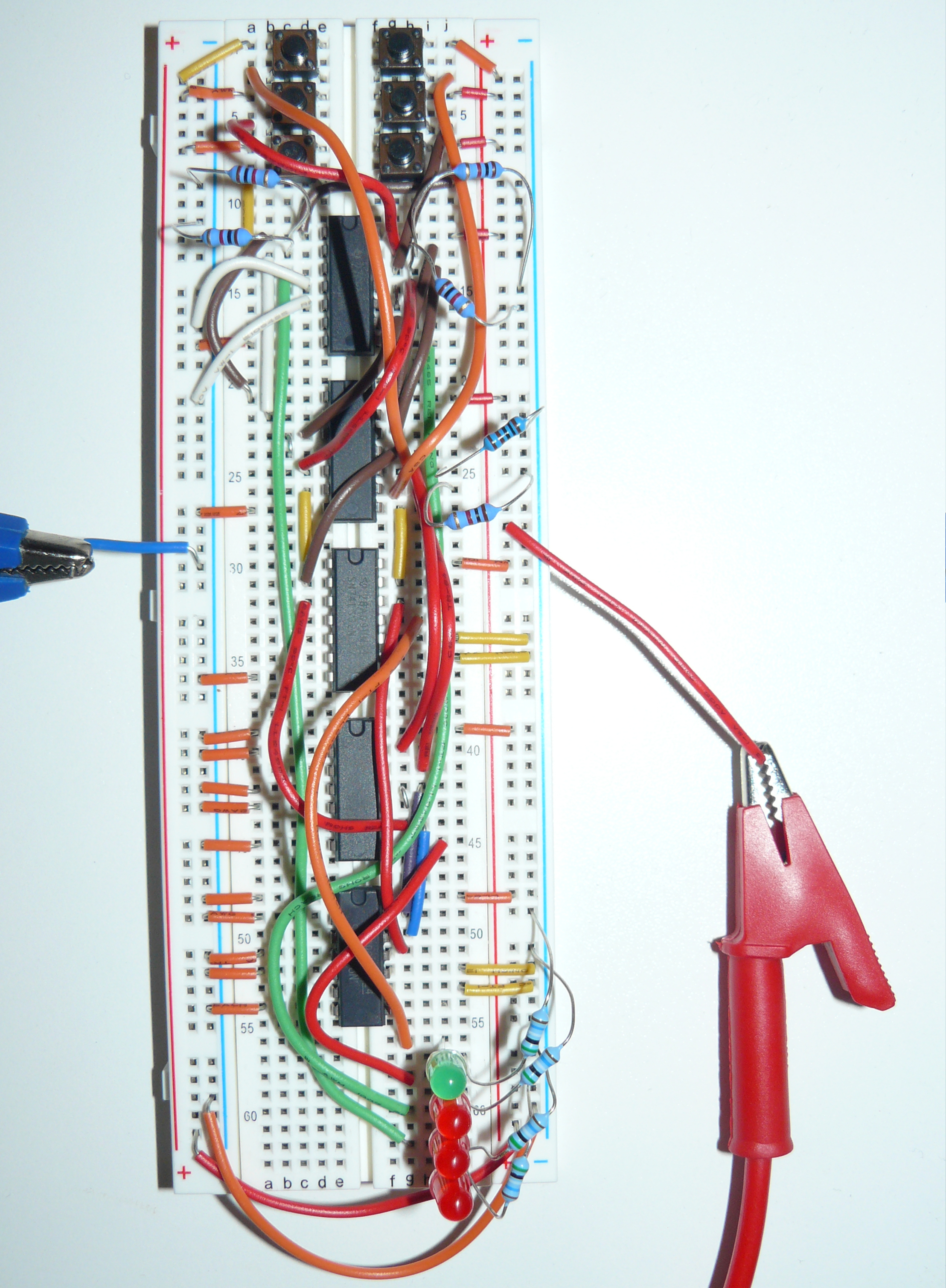
As we need 5x XOR and 5x AND gates, we will requires two of the 74LS86 and 74LS08 parts. Some of the gates on the chips will be unused. The circuit is constructed on a “breadboard” which is a board featuring spring loaded connections and is commonly used for prototyping. The exact layout and wiring on a breadboard is as follows:

The breadboard has a long connection (or rail) on either side for positive voltage and ground. The two positive rails and two ground rails are connected together. There are two columns of rows of pins. Each row of pins in the same column are connected together. The chips straddle the two columns such that opposite side legs are isolated from each other as they are on different rows.
Each chip requires power and ground. On the 7400 series, pin 14 (top right) is power (VCC) and pin 7 (bottom left) is ground. To get the chip the right way up, look for a notch at the top. Where a gate within a chip is unused, the inputs are connected to ground. This is not absolutely necessary but is generally considered good practice as they could potentially interfere with the operating gates if left floating (although in this case probably wont).
The circuit should be powered from 5V and in this case a power supply unit was used. However, if an appropriate power supply is not available it is possible to use batteries. The circuit can work on 4.5V as this is within the range of tolerance of the chips, therefore 3 x 1.5V (e.g. AA size) batteries wired in series could be used instead as long as the batteries are in good condition and putting out the full voltage.

The two 3-bit numbers to be added are input by holding down the relevant combination of buttons in binary. The left hand three switches are one number and the right hand three switches are the second number to be added. The lower switch is the least significant bit and the upper switch is the most significant bit. In this project momentary push switches have been used and as such the buttons need to be held down, however it would be an improvement to use switches that latch into position (like a light switch).
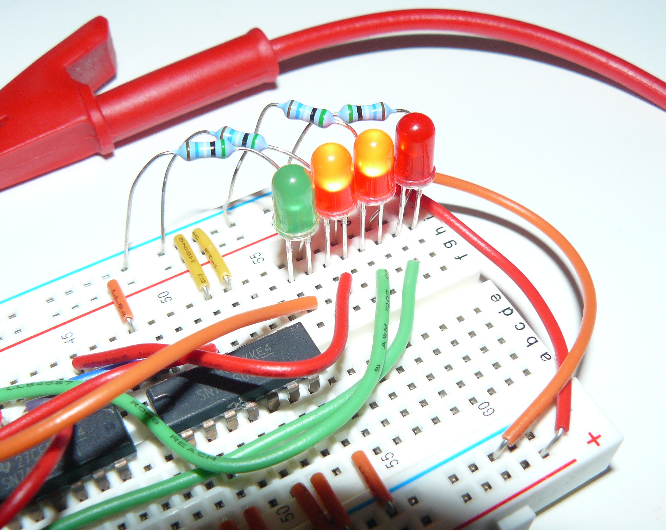
The LEDs displaying the result of a calculation are shown below. The right most LED is the least significant bit. The left hand (green) LED is the most significant bit which results from the final carry.

The circuit can be extended to handle larger binary numbers with more bits by chaining additional full adders on the end. There are enough logic gates left over in the above example to implement one more full adder and make it a 4-bit calculator.
Next: Add a decimal display to the adder project.
